The proposal emphasizes that as the key components of semiconductor production equipment, the R&D and production of precision ceramic components directly affect the development of semiconductor equipment manufacturing industry and even the entire semiconductor industry chain. It can be said that precision ceramic components are the foundation of the entire semiconductor industry. Therefore, whether from the perspective of economic security or industrial cost, in order to break through the “neck” dilemma faced by China’s semiconductor industry, we must pay attention to the localization development of key components of semiconductor production equipment such as precision ceramic components.
1、 Application of precision ceramics in semiconductors
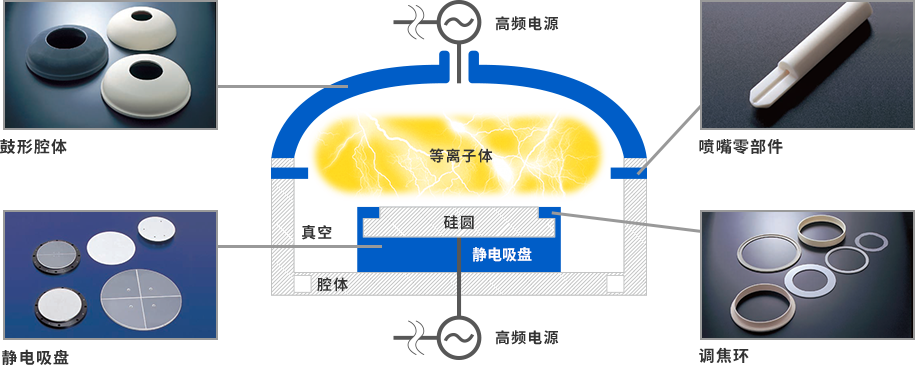
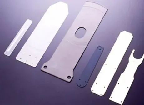
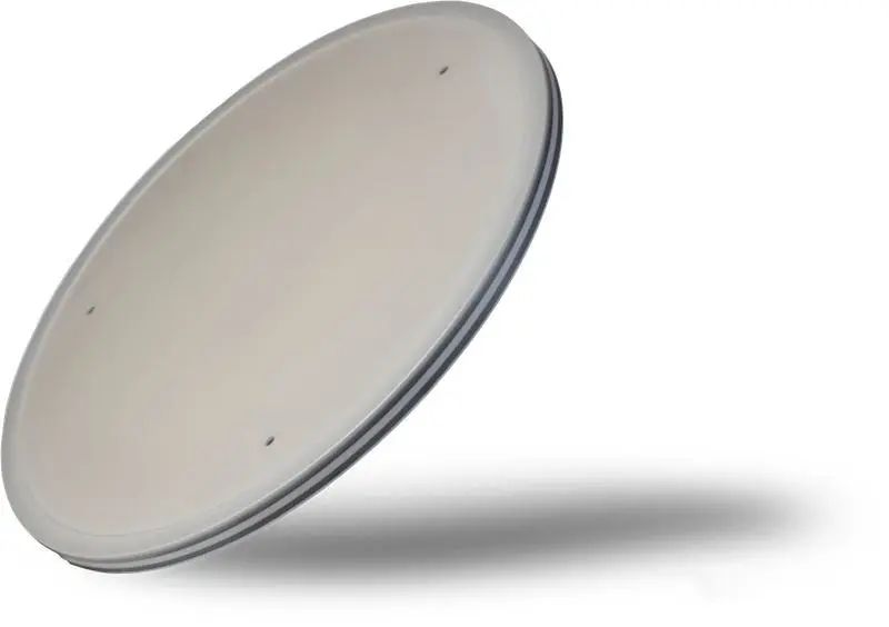
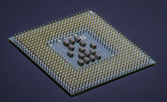
Semiconductor devices require a large number of precision ceramic components. Due to the advantages of high hardness, high elastic modulus, high wear resistance, high insulation, corrosion resistance and low expansion, ceramics can be used as parts of silicon wafer polishing machine, epitaxial/oxidation/diffusion heat treatment equipment, lithography machine, deposition equipment, semiconductor etching equipment, ion implanter and other equipment. Semiconductor ceramics include alumina, silicon nitride, aluminum nitride, silicon carbide, etc. in semiconductor equipment, the value of precision ceramics accounts for about 16%.
1. Alumina(Al₂O₃)
Alumina is the most widely used precision ceramic material in semiconductor equipment. It has the advantages of stable material structure, high mechanical strength, high hardness, high melting point, corrosion resistance, excellent chemical stability, high resistivity and good electrical insulation performance, and is widely used in semiconductor equipment.
In the semiconductor etching equipment, the chamber material of the etching machine is the main source of wafer pollution. The influence of plasma etching on it determines the yield, quality, stability of the etching process and so on. Therefore, it is particularly important to select the materials for the chamber of the etching machine. At present, high-purity al ɑ o ₃ coating or Al ɑ o ₃ ceramics are mainly used as protective materials for etching cavities and components in cavities. In addition to the cavity, alumina ceramics are also required for the gas nozzle, gas distribution plate and fixed ring of the plasma equipment.
In the handling of wafer silicon wafer, it will be applied to the ceramic manipulator made of alumina ceramics. Alumina ceramics and silicon carbide ceramics have the physical properties of compactness, high hardness and high wear resistance, as well as good heat resistance and excellent mechanical strength. In high temperature environment, they still have good insulation, good corrosion resistance and other physical properties. They are excellent materials for making mechanical arms of semiconductor equipment. In terms of material properties, silicon carbide ceramics are more suitable for making ceramic manipulator, but in terms of material price, processing difficulty and other economic aspects, alumina ceramic manipulator is more cost-effective.
In addition, alumina ceramics can be widely used in wafer polishing process, such as polishing plate, polishing pad correction platform, vacuum chuck, etc.
2. Silicon carbide (SIC)
Silicon carbide has high thermal conductivity, high temperature mechanical strength, high stiffness, low thermal expansion coefficient, good thermal uniformity, corrosion resistance, wear resistance and other characteristics. Silicon carbide can still maintain good strength at extreme temperatures up to 1400 ℃. The grinding disc made of silicon carbide ceramics has high hardness and low wear, and its thermal expansion coefficient is basically the same as that of silicon wafer, so it can be ground and polished at high speed.
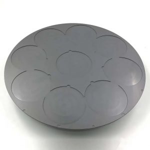
In the production of silicon wafer, it needs high-temperature heat treatment, and it is often transported by using silicon carbide fixture. It is heat-resistant and non-destructive, and can be coated with diamond-like carbon (DLC) and other coatings on the surface, which can enhance performance, alleviate wafer damage, and prevent pollution diffusion. In addition, SiC ceramics can also be used in XY platform, base, focusing ring, polishing plate, wafer chuck, vacuum chuck, handling arm, furnace tube, crystal boat, cantilever paddle, etc.
3. Aluminum nitride (AIN)
High purity aluminum nitride ceramics have excellent thermal conductivity, heat resistance, insulation, thermal expansion coefficient close to silicon, excellent plasma resistance, and uniform heat distribution. It can be applied to heater for wafer heating, electrostatic chuck, etc.
4. Silicon nitride(Si3N4)
Silicon nitride (Si3N4) is a material with high fracture toughness, strong heat shock resistance, high wear resistance, high mechanical strength and corrosion resistance. It can be applied to the platform, bearing and other parts of semiconductor equipment.
2、 Development status of precision ceramics at home and abroad
Recently, the American Semiconductor Industry Association (SIA) said that global chip sales reached a record $555.9 billion in 2021, an increase of 26.2% over the previous year. The association predicts that global chip sales will increase by 8.8% in 2022 as chip manufacturers continue to expand capacity to meet demand.
It is understood that after a year-on-year increase of 17% in 2020 and 39% in 2021, the equipment expenditure of wafer plants is expected to continue to grow in 2022. Semi (International Semiconductor Industry Association) pointed out that in 2022, the global expenditure on front-end fab equipment (excluding the front-end process equipment for packaging and testing, generally wafer manufacturing equipment) is expected to exceed 98billion US dollars, reaching a record high, and achieving growth for the third consecutive year.
Precision ceramics have become the key components of semiconductor equipment, accounting for more than 10% of the cost.
In high-end lithography machines, in order to achieve high process accuracy, it is necessary to widely use ceramic parts with good functional complexity, structural stability, thermal stability and dimensional accuracy, such as e-chuck, vacumm chuck, block, magnetic steel framework water-cooled plate, mirror, guide rail, etc. these key parts generally use precision ceramic materials.
In the etching equipment, the chamber material of the etching machine is the main source of wafer pollution. The influence of plasma etching on it determines the wafer yield, quality, and the stability of the etching process. Therefore, the research and development of an extremely etching resistant cavity material has become a very challenging task in the semiconductor integration industry and plasma etching technology. At present, high-purity al ɑ o ₃ coating or Al ɑ o ₃ ceramics are mainly used as protective materials for etching cavities and components in cavities. In addition to the cavity, precision ceramics are also required for the gas nozzle, gas distribution plate and fixed ring of the plasma equipment.
A semiconductor device seems to be made of metal and plastic, but in fact, there are many highly technical precision ceramic components hidden inside. In short, the application of precision ceramics in semiconductor equipment is far more than we expected.
2. Current global competitive landscape
At present, Kyocera of Japan, coorstek of the United States and bellinerglas of Germany are leading companies in the R&D and application of precision ceramic structural parts for IC core equipment. Kyocera and coorstek occupy 70% of the market share of high-end precision ceramic structural parts for IC core equipment.
The high-end ceramic components manufactured by Kyocera and coorstek have the characteristics of complete material system, excellent performance, complex structure and high machining accuracy. The precision ceramic components manufactured by Kyocera and coorstek almost cover the existing structural ceramic material systems, such as aluminum oxide, silicon carbide, silicon nitride, aluminum nitride, etc; The application field of structural parts also covers almost all the core equipment of integrated circuits, forming a series of precision ceramic structural parts with complete models and various varieties. For example, coorstek can provide a series of products such as special components for photolithography machine, special components for plasma etching equipment, special components for pvd/cvd, special components for ion implantation equipment, special components for wafer adsorption, fixation and transmission, etc; Kyocera can provide precision ceramic structural parts for equipment such as photolithography machine, wafer manufacturing equipment, etching machine, deposition equipment (CVD, sputtering), LCD, etc. China started late in the R&D and application of precision ceramic structural parts for IC core equipment. There are many key technical problems to be solved in the preparation of structural ceramic parts with large size, high precision, hollow, closed hole and lightweight structure.
3. Problems facing China
The “proposal on further accelerating the development of semiconductor precision ceramic components industry” proposed by the Central Committee of the Taiwan Alliance pointed out the problems existing in the development of China’s precision ceramic industry and gave important suggestions. Among them, there are the following problems in the development of China’s precision ceramic industry:
First, the R&D system is not perfect, and the core enterprises with R&D strength are absent for a long time. In terms of scientific research, although Tsinghua University, Shanghai Institute of silicate, Chinese Academy of Sciences and other scientific research institutions have a good accumulation in the research and development of precision ceramics, the R&D investment has almost stopped since the late 1990s, the application of precision ceramics has narrowed, and high-end products have stopped in the laboratory and are difficult to produce in mass. At the enterprise level, the ceramic industry chain has been large but not strong for a long time. In particular, the preparation level of ceramic powder in the raw material link is still far behind that in Japan and Germany. At present, domestic structural ceramics are basically limited to a large number of low-end ceramic products, and the scale is not prominent, so it is difficult to have sufficient R&D strength.
Second, domestic semiconductor system, manufacturing and packaging test manufacturers habitually purchase foreign equipment and components, and it is difficult for domestic components and materials to enter the procurement system. Domestic component products are in a critical period of exploration and improvement, and it is difficult to pass the OEM quality certification of equipment leading enterprises in the short term, which requires the patient participation and joint cultivation of key enterprises in the domestic semiconductor industry chain.
Third, the industrial input of key materials needs to be strengthened. Due to factors such as long R&D cycle and great development difficulty, at present, the industry investment in key materials such as precision ceramic parts is insufficient. Taking the National IC industry fund as an example, the investment in the equipment and materials industry accounts for only 3% of its total investment, which does not match its status and role.
3、 Suggestions on the development of precision ceramic industry in China
1. Cultivate potential enterprises and play a leading role in the industry.
It is suggested that the relevant departments of the state should further increase the support for the R&D and industry of precision ceramic components in the implementation of the outline for promoting the development of the national integrated circuit industry. By integrating the scientific research system with industry associations and alliances, a number of potential enterprises with international competitiveness will be selected and fostered in priority by concentrating resources nationwide, so as to drive the development of enterprises in the whole industry.
2. Strengthen industrial coordination and integrate domestic industrial resources.
It is suggested that the relevant national departments should encourage large-scale enterprises such as state-owned equipment, materials and chemicals to participate in the development of precision ceramics industry. Formulate the guiding objectives for the localization of equipment and accessories, establish a guidance mechanism for the localization of key components and materials that combines financial guidance with science and technology insurance, and encourage domestic semiconductor equipment enterprises to purchase domestic precision ceramic components through the support of government finance and market-oriented insurance products. Encourage enterprises and colleges to jointly establish technology R&D and testing certification institutions, and accelerate the establishment of a scientific and technological service system for the localization of key components and materials such as precision ceramics.
3. Strengthen enterprise related security and optimize the industrial development environment.
It is suggested that the relevant national departments should set up an intellectual property assistance center in the precision ceramic industry cluster to guide and assist enterprises to deal with intellectual property disputes and protect the driving force of R&D and innovation by shortening the intellectual property review and authorization cycle and increasing the punishment of infringement. Attract key precision ceramic enterprises to settle in the bonded area, and relieve the current research and development cost pressure of the semiconductor industry through the differentiation of tax policies in limited areas. At the same time, focusing on the cultivation of professional and technical talents in precision ceramic enterprises, we should strengthen the overall coordination of policies, support local governments to do a good job in the settlement of core team members, children’s schooling, medical care and other supporting support, especially the service support of talent teams introduced from foreign leading enterprises.
4. Give play to the role of the market and increase industrial investment.
It is suggested to further improve the trading functions of Shanghai Stock Exchange and Shenzhen Stock Exchange, and take advantage of the new opportunity of the establishment of Beijing stock exchange to innovate the establishment of new material plates such as precision ceramics in three national exchanges to accurately support small and medium-sized enterprises with core competitiveness in new materials. Encourage insurance, trust and other long-term funds to increase equity investment in outstanding unlisted small and medium-sized enterprises, open up reasonable channels for capital integration and withdrawal, and speed up the growth of new materials “hard core technology” enterprises.
The policy of "quality first, first-class service" has established a good image among users in many industries across the country. With professional technical strength and advanced management mode, we gather the strengths of many families, leverage our own advantages, and move forward at a better, newer, and faster pace
Copyright © 2023 Ultrafine Powder & New Materials Company. All Rights Reserved. ZHE ICP:2023013775